Nanoveu Accelerates 16nm Edge AI Chip Fabrication with Global Engineering Push
Nanoveu Limited advances its proprietary 16nm ECS-DoT chip fabrication, targeting completion by Q4 2025, supported by a strategic partnership and expanded engineering teams across multiple continents.
- 16nm ECS-DoT chip fabrication on track for Q4 2025 using TSMC’s FinFET process
- Strategic partnership with Center for Nanoelectronics and Devices enhances engineering capabilities
- 24-member multidisciplinary engineering team driving full-stack chip innovation
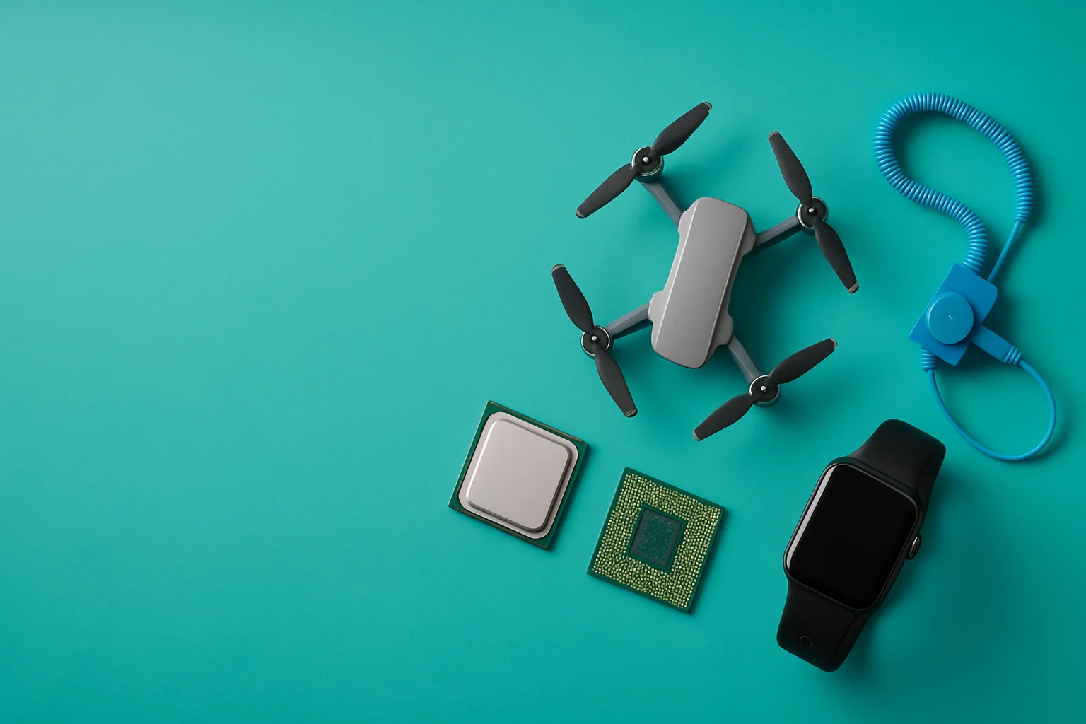
- Transition to compact Ball Grid Array packaging for wearables, drones, and IoT devices
- Software development teams expanding in Egypt and Singapore to support embedded AI
Nanoveu’s Strategic Leap in Semiconductor Innovation
Nanoveu Limited (ASX – NVU) has unveiled significant progress in the development of its next-generation 16nm ECS-DoT chip, a critical advancement in ultra-low power edge AI hardware. The company is targeting fabrication completion by the fourth quarter of 2025, leveraging Taiwan Semiconductor Manufacturing Company’s (TSMC) advanced 16nm FinFET process. This milestone marks a pivotal step in Nanoveu’s ambition to cement its position in the global semiconductor landscape, particularly within the burgeoning edge AI and IoT sectors.
Harnessing Top-Tier Talent Through Strategic Partnerships
Central to this progress is Nanoveu’s strategic collaboration with the Center for Nanoelectronics and Devices (CND), which provides access to a highly skilled regional engineering talent pool while maintaining cost efficiencies. The partnership has enabled the assembly of a 24-member engineering team spanning senior PhD-level experts, seasoned industry engineers, and emerging talent. This multidisciplinary team is driving full-stack innovation, covering analog, digital, and embedded system design, ensuring the ECS-DoT chip is optimized for power efficiency and AI performance.
Innovations in Chip Design and Packaging
The analog engineering division is focused on developing in-house wireless circuitry, analog-to-digital and digital-to-analog converters, and power management units essential for ultra-low-power communication. Meanwhile, the digital team is pushing boundaries with AI-optimized, memory-centric architectures and full system-on-chip (SoC) designs aimed at delivering intelligent decision-making capabilities at the edge with minimal latency and power consumption.
Complementing these design efforts, Nanoveu is transitioning the ECS-DoT platform to Ball Grid Array (BGA) packaging. This advanced packaging technique significantly reduces the chip’s footprint, enabling integration into compact devices such as drones, wearables, and IoT sensors, markets where space and power efficiency are paramount.
Expanding Software Capabilities to Support Market Readiness
Recognizing that hardware innovation must be paired with robust software, Nanoveu is expanding its embedded systems and edge AI software teams in Egypt and Singapore. These teams will focus on device firmware, system software integration, and application enablement, ensuring the ECS-DoT chip ships with a comprehensive software stack that enhances adoption readiness and customer compatibility.
Commercial Momentum with Current 22nm ECS-DoT Chip
While the 16nm chip is in development, Nanoveu is already commercializing its current 22nm ECS-DoT chip. The company is expanding its sales presence in the US and Europe and engaging early with original equipment manufacturers (OEMs) in wearables and drones. Early feedback and design wins suggest strong market interest, positioning Nanoveu well for volume production and broader adoption as the next-generation chip approaches fabrication.
Looking ahead, Nanoveu’s roadmap is ambitious, targeting applications across autonomous drones, smart wearables, edge healthcare, industrial IoT, robotics, and defense. The company’s integrated approach, combining cutting-edge silicon design, advanced packaging, and global software development, positions it to be a formidable player in the evolving edge AI ecosystem.
Bottom Line?
Nanoveu’s 16nm ECS-DoT chip development and global engineering expansion set the stage for a transformative leap in ultra-low power edge AI solutions.
Questions in the middle?
- What are the expected timelines for volume production and revenue generation from the 16nm ECS-DoT chip?
- How will Nanoveu’s chip performance compare against competitors in the ultra-low power edge AI market?
- What specific OEM partnerships are in place or anticipated to drive adoption of the new chip?